Graduate Research
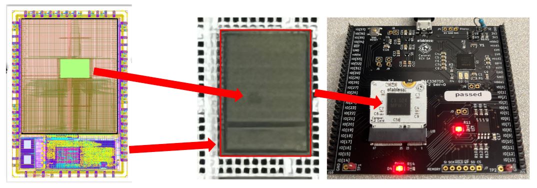 Ending in Fall 2024, I completed my Creative Component graduate research with Dr. Henry Duwe at Iowa State University, partnered with Gregory Ling. As part of my work, I had the opportunity to continue working on open-source ASIC design, utilizing the same open-source process supported by eFabless on the SkyWater 130nm technology. As part of my work, I helped document the digital and analog ASIC design flows required by eFabless to generate tapeout ready submissions. Additionally, I provided tutorials and guides on how to step through simple design for both design flows. In terms of deliverables, I was expected to submit an approved research paper to Iowa State University’s digital library, as well as a 45-minute oral exam to my major professor, Dr. Duwe. Attached are both the presentation and paper that I submitted for my final deliverables. By the end of our research, we were able to successfully establish Iowa State’s first ASIC design club, ChipForge, and provide them with all the necessary tools to create a tapeout ready design.
 Deliverables
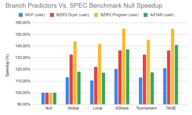 For my final project in CPRE 581, Computer Systems Architecture, me and two friends from solar car worked on analyzing different branch predictors for an open-source out of order processor, the BOOM core. Our motivation for this project was to further analyzer different branch predictors in the context of area, power, and slack synthesis results for a real FPGA hardware application. Most of the research papers we reviewed in the class were solely focused on prediction accuracy or performance in terms of execution time, with little consideration for area or power consumption. The goal of our paper was to use the open-source framework Chipyard to generate an out of order processor core which could be instantiated on an FPGA to synthesize and reconfigure our multiple BOOM cores with varying branch predictor configurations, such as tournament, GShare, Local, or more.
 Deliverables
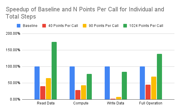 SmartSSD is a Computational Storage Device that includes a 4TB Samsung NAND SSD device and a Xilinx Kintex Ultrascale FPGA in one package. This device can act as a normal storage device to the host, directly interfacing between the host and FPGA like a normal accelerator, or between the SSD device and FPGA to utilize low latency memory transactions by using a PCIe switch within the SmartSSD device. As part of a semester long project for a graduate course at Iowa State University, CPRE 563, me and a partner developed an accelerator design for SmartSSD which would be targeted towards neural network image inferencing. The goal was to utilize the high bandwidth, low latency memory transactions directly between the SSD and FPGA devices, while synthesizing an accelerated FPGA kernel by utilizing Vitis HLS with C++ code for a multiply and accumulate function, which could be used to generate convolution points for a neural network inference.
 Deliverables
Machine Learning
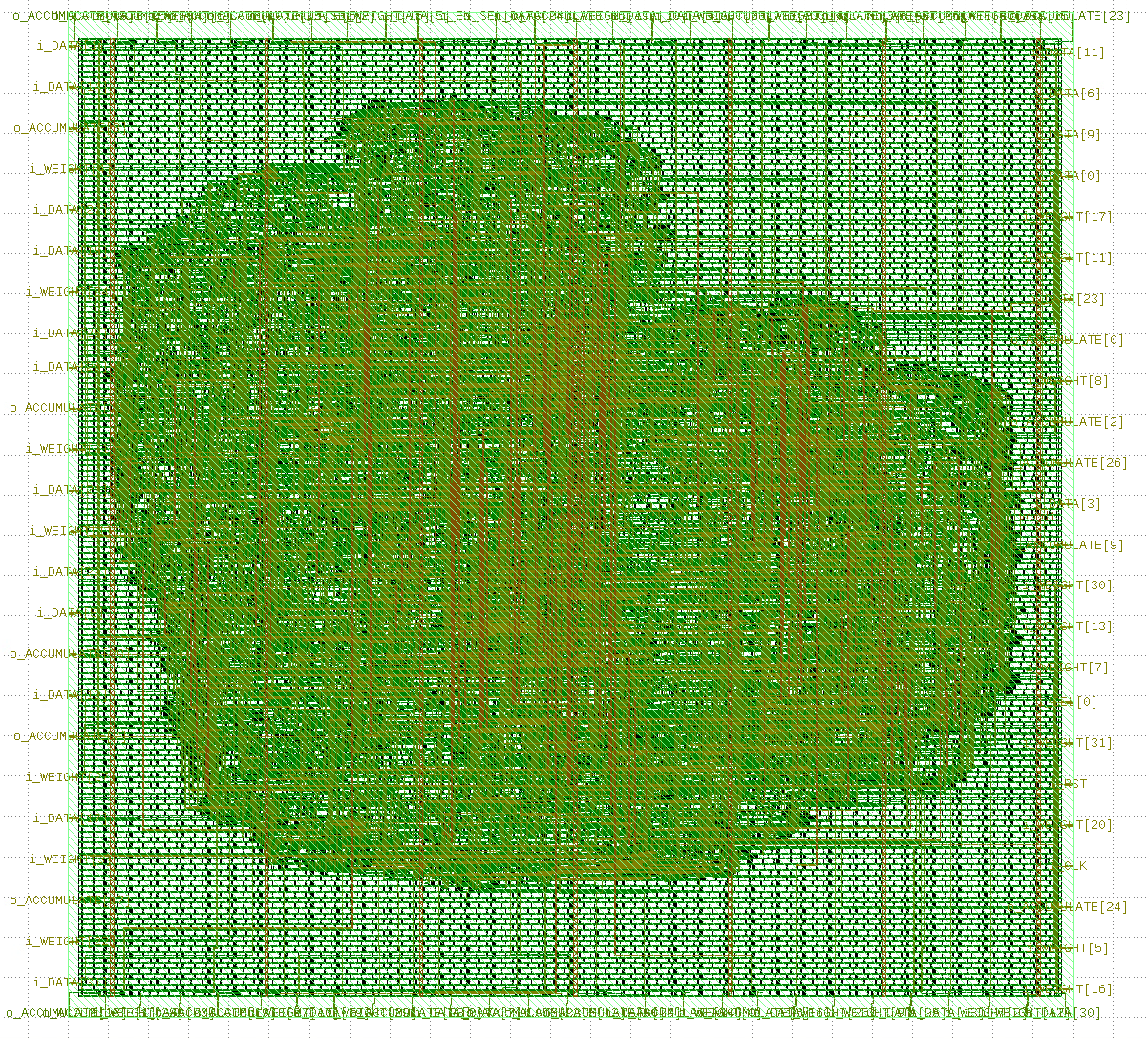 In Fall 2024, I took my last class at Iowa State University as apart of my Computer Engineering graduate degree. The course was focused on hardware applications of machine learning systems, and throughout 6 different labs a partner and myself integrated a image inference convolutional neural network in python, C++, and in Verilog utilizing a Xilinx FPGA and Digilent ZedBoard. As part of our final project, we created a multiply accumulate module that was synthesized and constrained with the same open-source digital ASIC design process I utilized for senior design and graduate resource. This enabled us to create a design for a future ASIC tapeout that my partner can verify in person in the Spring 2025 semester. As part of the design process, we defined our design, created an automated suite of tests, and helped integrate the design into the final tapeout submission. The included image on this page is the GDSII layout of our design cell in the open source SkyWater 130nm process.
 Deliverables
FPGA Task Scheduler
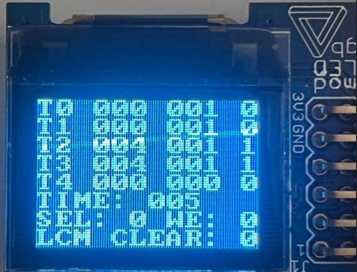 In the Fall 2023 semester, I took CPRE 558, Real Time Operating Systems, at Iowa State University. As a final project, me and a partner decided to create a hardware implementation for a periodic RMS scheduler using Verilog RTL and an FPGA implementation. The goal of this project was to design a hardware architecture that could achieve faster and more efficient context switching for tasks in comparison to a software scheduler that was intended for the same task set.
 Our design was centered around the 5 stage MIPS processor that we designed in a previous computer architecture course, where we could use existing code such as a register file or program counter as a baseline. The central idea was that we would have a register file and program counter for each task, and have a control module which would switch between the five tasks based on if they were complete, missed their deadline, or were ready to be used. In the RMS protocol, the task with the lowest period has the highest priority, and is able to preempt currently running tasks when the period refreshes, meaning we had to enable this context switching in our control module. We also included a standard up counter to monitor the current time, as a reference for when each task should become active again. The main benefit of this design was that context switching could occur in a single cycle, which can be much more efficient than a software implementation, and could still be reconfigurable at compile time with the use of an FPGA instead of an ASIC.
Each designed module was tested functionally individually, and we followed integration testing with Verilog testbenches also. When that was complete, we integrated our design onto my Basys 3 FPGA Development board, which has a Xilinx Artix-7 FPGA board. Using the OLED display interface I designed in Summer 2023, we were able to create a display monitor to show the state of each task, including its stored register value, computation time, and if it was complete. Alongisde this, we displayed the current time, which task was currently active, and if the time was at the least common multiple of all task periods, meaning the entire schedule would reset. This design proved the feasibility of a hardware based task scheduler on a reconfigurable FPGA, and further work could be done in comparison to software schedulers in terms of context switching, power consumption, area requirements, timing, and design time.
Deliverables
Least Significant Bit Steganography for 2D Image Applications
The overall code process was very similar for hiding different types of media within 2D images. We first began by writing text files, by reading out every char and breaking it down bit by bit. We utilized a 3 level nested for loop to clear and set N bits, to be set with the 1D array of bits from the text file. We found that with an N value of 3 or more, the original image to hide data within started to become noticeably corrupted. Despite this, it still was possible to fully recover the hidden media. A similar process was followed for hiding 2D images, which just involved updating how the images were formatted into a 1D array of bits from each pixel’s colors.
To further push our code, we explored writing data out as a bitstream, which allowed for higher amounts of compression due to how Windows compressed 2D images with lossless data. This allowed us to hide a direct copy of an image within itself, since we were reading the original image out uncompressed in MATLAB to hide it within. We also created a script to upscale the resolution of an image, which allowed us to fully hide the feature-length film of The Bee Movie within a picture of our friend Caden. This comparison can be seen below, with the full embedded movie hidden in the image to the right.
 To analyze the results of hiding media, we used the Structural Similarity Index, which compares the likeness of two images, in which we could compare the original image and the modified image with hidden contents, to see how similar they appeared to the eye. The Structural Similarity Index ranged from 0 to 1, with 1 being perfectly identical. We found that with the bitstream implementation we could not hide compressed text files, but could achieve a lower N value and higher similarity with 2D compressed image, due to lossless data loss with Windows image compression. This provided for some nice comparisons in both our report and presentation, can be seen below.
 Deliverables
OpenFPGA Research
For this research, I began by reading over the background research papers surrounding OpenFPGA and reading through their online documentation. I was able to learn more about what made up an FPGA fabric, and what different design considerations an engineer must make when determining the right FPGA architecture. This was extremely beneficial to me, since I have worked on developing RTL for FPGA’s for multiple years now, and it helped to give me a better understanding of place and route techniques after taking a digital VLSI course and my open-source digital ASIC fabrication senior design project.
I also spent some time working with the OpenFPGA git repository and tools directly. For this, I learned how to install the proper dependencies and build the git repo, alongside utilizing a Docker instance to run precompiled binaries for the toolflow. I ran multiple testbench configurations, and learned that OpenFPGA has two different types of testbench procedures which are fully automated. A user can provide functional Verilog benchmarks, which can be either reconfigured onto the FPGA in an initial configure mode or compared with a direct mapped netlist inside the FPGA. The testbench which requires flashing a bitstream takes much longer, but is useful to verify the FPGA fabric can generate a proper bitstream and generate the same matching output to a target functional Verilog benchmark. To run a testbench, I had to also generate an FPGA Verilog fabric netlist, in which multiple different XML files can be referenced to alter the FPGA architecture description.
Finally, I learned how to alter the cells referenced in the FPGA XML architecture description files. I ran through two documented processes for this, including using a custom functional Verilog module and an open-source cell from the same Skywater 130nm PDK that I utilized for my senior design project. Both of these Verilog designs can be referenced on the path directly in the XML files, and will then be able to be included for the proper module name when the total FPGA Verilog fabric netlist is generated through the OpenFPGA toolflow. This is extremely beneficial, since you can then use custom cells such as the open-source Skywater 130nm PDK, which can be carried through after synthesis for place and route generation and fabrication.